
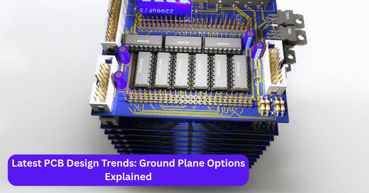
In the ever-evolving world of electronics, PCB design remains a critical foundation for device performance and reliability. For engineers and designers seeking cutting-edge solutions, understanding the latest trends in PCB ground plane options is essential. Whether you are working with high-speed digital circuits or sensitive analog systems, the choice and configuration of ground planes can significantly influence electromagnetic compatibility (EMC), signal integrity, and thermal management.
If you are exploring PCB design services or planning your next project, keeping updated on ground plane strategies is a must. Ground planes serve as a reference for signals, reduce noise, and provide a path for return currents. With the complexity of modern PCBs growing, new approaches to ground plane implementation have emerged to meet design challenges in 2025 and beyond.
Understanding the Role of Ground Planes in PCB Design
Ground planes are continuous conductive layers within a PCB, typically copper, that act as a common electrical reference point for components and circuits. They play a pivotal role in stabilizing voltage levels and reducing electrical noise by minimizing ground loops and providing a low-impedance path for return currents.
In PCB design services, ground planes also enhance signal integrity by reducing crosstalk between adjacent traces and lowering electromagnetic interference (EMI). Moreover, ground planes assist in heat dissipation, improving thermal management of power-dense components.
Common Ground Plane Configurations
PCB ground plane configurations vary based on the application and complexity of the circuit. The most common types include:
- Solid Ground Planes: A continuous copper layer covering the entire PCB layer, providing maximum shielding and lowest impedance paths.
- Split Ground Planes: Dividing the ground plane into sections for different circuit domains, like analog and digital grounds, to reduce interference.
- Cross-Hatched Ground Planes: A mesh or grid pattern of copper traces instead of solid copper, intended to balance cost and performance.
Among these, solid and cross-hatched planes are widely discussed in PCB design for their trade-offs in manufacturing costs, electrical performance, and thermal behavior.
Benefits and Drawbacks of Different Ground Plane Types
Solid Ground Planes offer excellent electrical performance due to the continuous conductive surface. They minimize ground impedance and provide optimal shielding against EMI. However, solid copper planes can introduce thermal challenges, especially in multilayer boards, because they retain heat, sometimes leading to hotspots.
Cross-Hatched Ground Planes reduce copper usage and cost by creating a grid-like pattern rather than a solid fill. This can improve thermal dissipation by allowing better airflow within the PCB layers. However, the cross-hatched pattern may increase ground impedance and EMI susceptibility compared to solid planes. Despite this, recent advances in design software and manufacturing allow optimized cross-hatching that meets high-frequency and thermal requirements.
Split Ground Planes are used when isolation between different circuit sections is necessary, but improper implementation can cause return current discontinuities, leading to noise and signal integrity issues.
Current Trends in Ground Plane Design for PCBs
Modern PCB design are embracing hybrid approaches that blend the benefits of different ground plane styles. These trends are driven by advancements in high-frequency circuit demands, miniaturization, and cost-efficiency:
- Adaptive Cross-Hatching: Unlike traditional uniform grids, adaptive cross-hatching uses variable spacing and thickness to optimize electrical and thermal performance. This method balances copper savings and ground integrity more effectively than earlier techniques.
- Multilayer Ground Planes: With increasing PCB layer counts, designers place multiple solid ground planes interleaved with power planes and signal layers to improve shielding and reduce EMI. This multilayer approach also helps in managing high-speed signals by providing well-defined return paths.
- Integrated Thermal Management: Ground planes are increasingly designed with thermal vias and optimized copper thickness to dissipate heat efficiently from power components. This trend supports reliable operation of dense and high-power PCBs.
- EMC-Focused Grounding Strategies: To comply with stricter electromagnetic compatibility regulations, designers carefully plan ground planes with segmented or controlled splits, ensuring continuous return paths for high-speed signals.
Importance of Proper Ground Plane Selection in PCB Design Services
Choosing the right ground plane configuration is a fundamental decision in PCB design that affects overall system reliability, manufacturability, and cost. For example, solid ground planes may increase manufacturing complexity and expense but provide superior electrical performance for RF or high-speed digital designs.
Conversely, cross-hatched planes offer cost savings and thermal benefits, which can be critical in large or power-intensive boards. However, these must be carefully engineered to avoid EMI and signal integrity issues.
Designers today often rely on simulation tools to model ground plane behavior and validate designs before fabrication, ensuring the chosen approach meets the performance requirements.
Interlinking Insight: Cross-Hatching in PCB Ground Planes
A notable aspect of ground plane design gaining attention is the technique of cross-hatching. This involves using a grid-like copper pattern instead of a solid plane, which can balance thermal dissipation and manufacturing cost. Cross-hatching is especially useful in multilayer boards where heat buildup is a concern.
For a detailed understanding of cross-hatching, including its advantages, disadvantages, and design tips, check out this in-depth resource on PCB Cross-Hatching. This guide offers valuable insights for engineers and designers who want to optimize their PCB ground planes effectively.
PCB Design Services and Ground Plane Optimization
When engaging professional PCB design services, ground plane selection is a crucial consultation point. Experienced designers assess the following factors to recommend the best ground plane solution:
- Circuit Type and Frequency: High-frequency RF circuits often benefit from solid ground planes, while lower frequency or mixed-signal boards may use hybrid approaches.
- Thermal Requirements: Power electronics and high-current boards require ground planes designed for efficient heat spread and dissipation.
- EMC Compliance: Regulatory standards demand careful grounding to minimize emissions and susceptibility.
- Cost and Manufacturability: Budget constraints influence whether solid or cross-hatched planes are preferable.
By addressing these elements, PCB design ensure the final product achieves performance, reliability, and cost-effectiveness.
Best Practices for Ground Plane Implementation
To maximize ground plane effectiveness, designers follow several industry best practices:
- Ensure Continuous Ground Paths: Avoid breaks in ground planes, especially in return paths for high-speed signals, to prevent EMI and signal integrity problems.
- Use Ground Vias Strategically: Proper placement of ground vias connects different ground layers, improving current return and shielding.
- Minimize Split Ground Planes: Where possible, avoid splitting ground planes as this can cause ground loops and increase noise.
- Simulate Early and Often: Use electromagnetic simulation tools to predict ground plane performance and adjust layouts proactively.
- Incorporate Thermal Vias: When heat dissipation is critical, integrate thermal vias that connect ground planes to internal copper layers or heat sinks.
These techniques ensure the ground plane delivers both electrical and thermal benefits as intended.
Future Outlook: Evolving Ground Plane Designs
The future of PCB ground plane design will continue evolving alongside electronics trends. As device speeds increase and designs shrink, ground planes must adapt to tighter layouts, more complex multilayer stacks, and emerging materials.
Innovations such as conductive polymers, embedded heat spreaders, and advanced copper treatments may redefine how ground planes are constructed. Moreover, AI-driven design tools could optimize ground plane patterns automatically based on performance targets.
For now, understanding the fundamentals and latest trends in ground plane options remains essential for any successful PCB design.
Conclusion
Ground planes are the unsung heroes of PCB design, crucial for stable voltage references, EMI control, signal integrity, and thermal management. In 2025, designers have multiple ground plane options—solid, cross-hatched, split, and hybrid—that balance electrical performance with cost and thermal needs.
When considering PCB design, paying close attention to ground plane strategies can significantly enhance your project’s success. Whether you choose solid copper or cross-hatching, ensure your design follows best practices and leverages the latest trends.
To deepen your knowledge on one of the popular ground plane techniques, don’t forget to explore this detailed article on PCB Cross-Hatching, a valuable resource for any PCB designer.