
In the world of electronics, the path from concept to commercial product is paved with intricate steps and detailed engineering. At the heart of many modern electronic devices lies the printed circuit board (PCB), a critical element that connects and supports electronic components. Before a PCB ever makes its way into a consumer product, it goes through rigorous stages of development. Among these, the transition from a PCB prototype to a final design is one of the most crucial — and often misunderstood — phases.
Understanding this transition is key for anyone involved in electronics design, from hobbyists to professional engineers. Let’s delve into the fine line between PCB prototypes and final designs, explore why it matters, and uncover how to navigate it effectively.
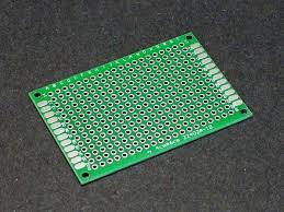
What is a PCB Prototype?
A PCB prototype is an early version of a circuit board that serves as a proof of concept for a specific design. It’s primarily used to test the functionality, performance, and feasibility of a proposed layout before mass production. These prototypes allow engineers and designers to identify potential flaws, make adjustments, and validate the design’s capabilities.
Prototypes can range from simple breadboards to more complex, fully fabricated PCBs that closely resemble the intended final product. Depending on the complexity of the project, multiple iterations of a prototype may be developed before the design is finalized.
Why PCB Prototyping is Essential
- Risk Reduction: Prototypes allow teams to identify design flaws and manufacturing issues early in the process. This prevents costly mistakes down the line.
- Performance Testing: Prototypes give a real-world platform to evaluate electrical performance, thermal behavior, and component compatibility.
- Design Validation: Before committing to a large production run, designers can confirm whether the board performs as expected under actual working conditions.
- Feedback Loop: Stakeholders, including engineers, marketers, and clients, can review the prototype and provide input, ensuring the product meets all functional and market needs.
If you’re considering your first prototype, you can Find Out More by consulting expert resources or prototype service providers. They can help guide your project through its earliest stages with the right tools and techniques.
The Characteristics of a Final PCB Design
Once a prototype has been tested, tweaked, and validated, the goal is to translate it into a final design. This version must be optimized not only for performance but also for manufacturability, cost-efficiency, and compliance with industry standards.
Key features of a final PCB design include:
- Manufacturing Readiness: The final design must be fully compatible with automated production processes, including pick-and-place machines, reflow ovens, and testing systems.
- Design for Manufacturability (DFM): Engineers use DFM principles to ensure the PCB can be reliably manufactured at scale without defects or inconsistencies.
- Compliance and Standards: Final PCBs must comply with international standards such as IPC, RoHS, and CE, depending on the application and geography.
- Cost Optimization: Component selection, board layers, and material types are all fine-tuned to balance performance and cost, a process not usually emphasized during prototyping.
If you’re still unsure about the specifics of transitioning to a production-ready PCB, you can check over here for detailed guidelines and best practices from industry leaders.
The Subtle Yet Crucial Differences
Though a prototype and a final design may look nearly identical at first glance, the devil is in the details. Here are some subtle but critical distinctions:
- Material Selection: While prototypes might use general-purpose FR4 material, final designs may require specialized substrates like polyimide or Rogers for high-frequency applications.
- Component Tolerances: Prototypes may be more forgiving, but final designs demand tighter tolerances to ensure reliability, especially in high-speed or mission-critical systems.
- Layout Optimization: A prototype may use a straightforward layout for simplicity. In contrast, final designs optimize trace widths, via placements, and power distribution to minimize interference and improve performance.
- Testing Routines: Final boards undergo automated testing such as AOI (Automated Optical Inspection), ICT (In-Circuit Testing), and functional testing. Prototypes often rely on manual testing and debugging.
To really understand the transition in detail, go right here to explore case studies and expert analyses that highlight how small design decisions make big impacts in production.
Bridging the Gap: Best Practices
Navigating the transition from prototype to final design involves a blend of foresight, technical expertise, and strategic planning. Here are some best practices:
- Document Everything: Maintain clear records of design changes, test results, and feedback. This ensures a smooth handoff between teams and phases.
- Use Scalable Design Principles: Even during prototyping, consider aspects like layout modularity, component availability, and design reuse to simplify the scaling process.
- Simulate Early and Often: Leverage simulation tools to anticipate issues in thermal behavior, signal integrity, and power distribution before fabrication.
- Partner with Experts: Engage with PCB manufacturers early to get input on design-for-manufacturing concerns. Their insights can help avoid production bottlenecks.
Conclusion
The journey from a PCB prototype to a final design is much more than just a cosmetic upgrade. It’s a transformation that ensures your electronic device not only works but can also be manufactured at scale, meet industry standards, and succeed in the marketplace.
By understanding the distinctions and following structured development processes, teams can reduce risk, improve performance, and streamline time to market. Whether you’re a startup developing a new IoT gadget or an engineer working on aerospace systems, acknowledging the fine line between these two stages can be the difference between a successful launch and a costly redesign.
To take your project to the next stage, Find Out More by consulting with experienced designers, leveraging advanced simulation tools, and engaging with trusted manufacturing partners. For deeper insights, you can check over here or go right here to access comprehensive resources on PCB development from prototype to production.